
The Ambient Thermal Electric Converter uses alternating materials that act as if they’re hot or cold.
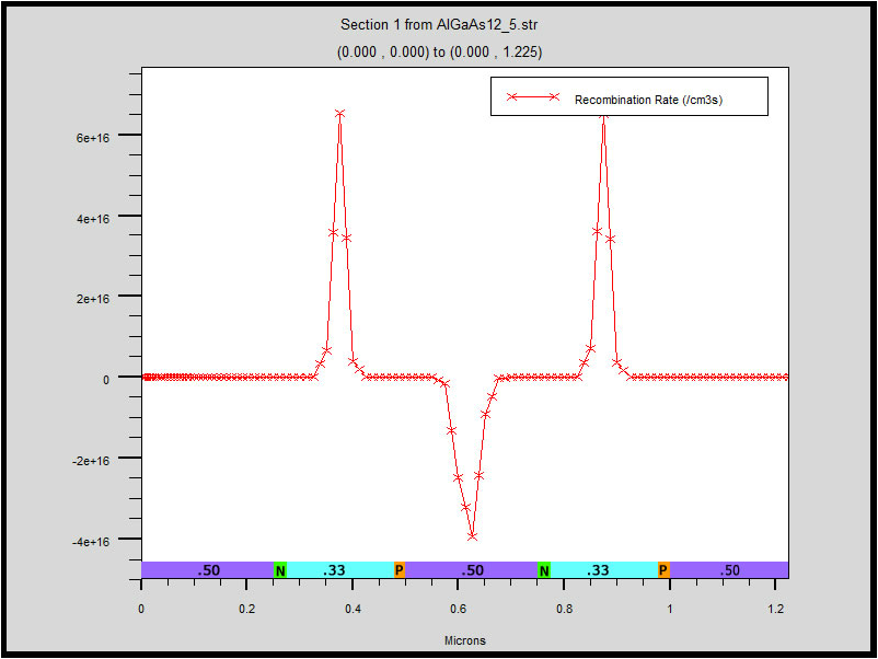
The graph above was produced by commercial semiconductor modeling software. It shows the net carrier recombination across the model. The ‘.50’ region in the center acts as if it is warmer than the ‘.33’ regions on either side. For this to continue, the generated carriers have to go somewhere. They flow to the recombination areas. Because the ‘n’ and ‘p’ layers are selective, electrons flow from right to left across the ‘n’ layer, with matching holes flow from left to right across the ‘p’ layer, effecting a current flow.
We can use this apparent temperature difference to generate power.
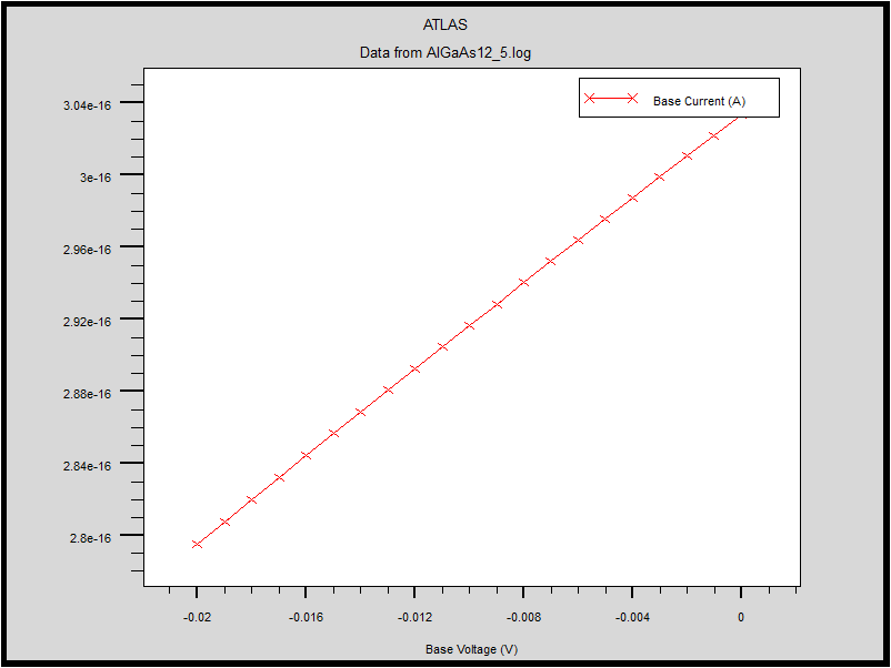
The graph above shows the bias current for the same model run with a reverse bias. Zero bias is at the far right. The modeled section is a 1 micron (1/1000 millimeters) cube. This is the same structure we tested, and closely matches current we measured.
A more detailed analysis is in the Test Results document, Section 3.