
We use pairs of materials that act like one is hot and the other is cold. We use that temperature difference to produce electricity.
It’s okay to stop reading here, but if you want to see more theory, read on.
The Ambient Thermal Electric Convertor (ATEC) converts heat into electricity. This introduction explains the key elements of this unique device to help anyone understand how it works.
The ATEC uses known properties of semiconductor materials and the behavior of electrons within these materials, along with a layered structure that creates channels for electrons. Heat pushes electrons through these channels, consuming the heat and giving us electricity we can use without any chemical or mechanical process. This is explained by:
- Defining the relevant behaviors of electrons
- Describing the relevant behaviors of semiconductor materials
- Showing how electrons move without channel restrictions
- Showing the effect of channel restrictions
- Showing the resulting channeled flow of electrons.
The following definitions provide only enough about its components to describe ATEC operation.
Atoms: All matter is made up of atoms, which consist of a central nucleus of neutrons and positively charged protons with negatively charged electrons in orbit around them.
Bound Electrons: Electrons in their normal state are in orbit around a specific atom, and are bound to that atom by the electromagnetic pull of its nucleus These are also known as valence electrons.
Free Electrons: These are electrons that have disengaged from their place around an atom and are traveling on their own. The electricity moving through electrical wires or coming out of flashlight batteries, for example, is carried as Free Electrons.
In metals, each atom almost always releases one or more electrons. In semiconductors, however, electrons disengage from atoms randomly, but at predictable rates based on the materials and their temperature.
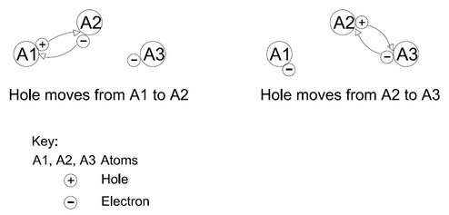
Holes: These are places in atoms that are left behind when Free Electrons break out of their places. A Hole can be treated as if it, too, is a thing. Atoms “trade” Holes as they trade Bound Electrons. In effect, Holes also move around at the same time as Bound Electrons do. For example:
Semiconductor: A semiconductor is a material, such as silicon, with electrical conductivity between an insulator (such as glass) and a conductor (such as copper wire). Semiconductors are basic components of various electronic devices such as cell phones and computers. Electrons in semiconductors are normally bound to atoms. Sometimes electrons are knocked loose by heat, light or radiation producing Free Electrons. This “knocking loose” leaves behind a Hole where an atom is missing an electron. Free Electrons and Holes, thus created in pairs, separate and can each recombine later into other atoms in a continual process.
Generation: In Semiconductor materials, as an electron is knocked loose, it and its matching Hole separate and wander around. The frequency of this Generation process depends upon the material and typically increases with temperature.
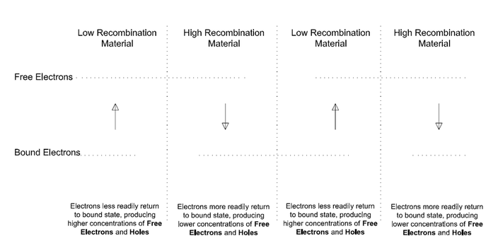
Recombination: Free Electrons and Holes interact with each other to recombine. The rate at which Recombination takes place varies by material. In some materials it is a simple process and therefore faster while in others it is more complex and slower. For example, recombination is much faster in Gallium-Arsenide than in Silicon This difference in Recombination rates is a critical feature of the ATEC that we exploit to create different concentrations of Free Electrons and Holes.
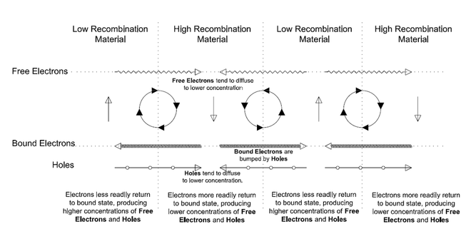
Junctions: An ATEC consists of layers of semiconductor materials. The region between layers is a Junction, also referred to as a Heterojunction. Adjacent layers have different properties, including different or unequal Recombination rates. Free Electrons and Holes tend to move across a Junction from one material to the other and recombine at a predictable rate. Electrons and Holes generated in the Lower Recombination rate material also tend to move across the Junction to the Higher Recombination rate material before recombining. They do this simply because there are more opportunities to recombine in the Higher Recombination rate material.
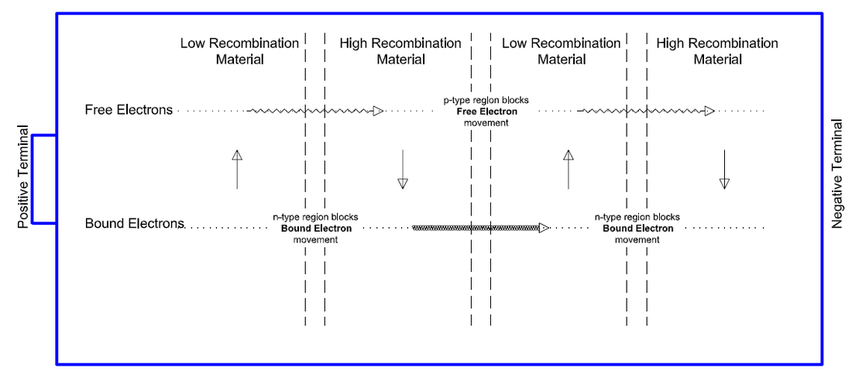
Doping: The Doping of Semiconductors adds an impurity to the material to change its electrical properties. It is used to either restrict or increase the movement of Free Electrons or Holes through a layer of material, effectively creating channels for Holes and Free Electrons. For example, Negative Doping (n-type) changes the material to add extra Free Electrons. This allows electrons to migrate from a Low Recombination material to a High Recombination material while blocking the flow of Holes. The effect is a net flow of electrons in that direction. Positive Doping (p-type) changes the material to have extra Holes and therefore it has the reverse effect on the movement.
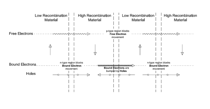
The effect of Doping is shown above. With Positive (p-type) and Negative (n-type) Doped layers between the Low Recombination and High Recombination layers as shown, the circular flows are broken. What remains are:
- Free Electrons flowing from left to right (still from the Low to High Recombination layers)
- Holes flowing from right to left (still from Low to High Recombination layers)
The net effect is a flow of Free Electrons from left to right and a flow of Holes from right to left that keeps the layers in balance, which is the electric current you want.
ATEC: This is the device that turns heat into electricity. This is achieved through the use of semiconductor materials, purposefully doped to provide a predictable rate of Generation, movement and Recombination across junctions between the materials. In this application, the more doped semiconductor materials used, the greater the flow of electrons in one direction. In the ATEC, the electron and hole pairs are generated in a lower recombination material and recombine in the higher recombination material (see picture below), channeled in a useful direction much like a funnel. As higher temperature is applied, the process generally becomes faster, thus increasing the electrical output.
The ATEC layers are assembled into a convenient package for particular applications. The following figure represents a common and easily recognizable package that we might use in a flashlight:
There are many other possible configurations for other applications. Output voltage is increased by adding more layers, in much the same way as stacking batteries increases the voltage. Increasing the temperature also generally increases the current. The maximum obtainable current depends on the size and thickness of the layers. Some consideration should be given to performance, which depends heavily on the materials used, the layering of the materials, and how they form their channels.
Summary
The ATEC converts heat into electricity by using the known properties of semiconductors wherein heat and differing Recombination rates cause different concentrations of Free Electrons and Holes. Heat pushes the Free Electrons and Holes through separate channels and Recombine, which creates an electric current.
Unlike an alkaline or lead-acid battery, the structure and materials of the ATEC are not consumed by the process. Instead, heat is consumed, leaving the structure unchanged. Replacing the consumed heat recharges the ATEC.